Electron microscopy is based on expertise from sample preparation to image analysis for a wide range of solid material. The focus is on materials science electron microscopy.
For an ever-deeper understanding of solid matter and small objects, characterization by means of electron microscopy (EM) is now an indispensable analytical method. It is impossible to imagine scientific laboratories without it. EM is an imaging technique and allows objects and structures to be imaged down to the nanometer scale. Secondary-, backscatter-, transmission- and diffraction-electrons can be detected, which contain different information about topography, morphology, material composition, structure and much more. In addition, the study of emitted characteristic X-rays can provide information about the local elemental distribution. In addition to imaging crystal structures down to atomic resolution and local imaging of chemical composition, EM has a wide range of applications. By using novel working methods such as electron tomography, three-dimensional models of materials can be imaged on the nanometer scale. Electron crystallography can be used to determine structures of single crystallites and enable the use of special sample holders for in-situ experiments at the nanometer scale.
Equipment
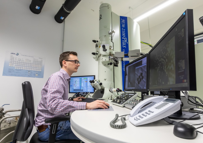
Transmission electron microscopy is performed on a JEM-2100Plus from Jeol at the Institute of Chemical Technology. This is a multifunctional analytical TEM. It is equipped with a LaB6 electron source and can be operated at 200 kV and 80 kV. The microscope allows imaging in TEM mode with a point resolution of up to 0.23 nm. It is equipped with an ultra-fast 4K camera system (CMOS, TVIPS), a STEM unit (bright and dark field detectors) and energy dispersive X-ray spectroscopy (EDX, EDAX) for highly sensitive chemical analysis. Additional accessories for tomography, electron crystallography and in-situ experiments (heating and cooling experiments) make the system suitable for a wide range of applications.
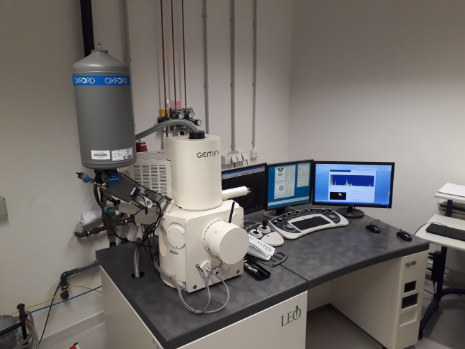
The faculty at the Institute of Mineralogy, Crystallography and Material Science (IMKM) has a LEO 1530 scanning electron microscope from Zeiss, equipped with a secondary electron, a backscatter electron, and an InLens detector for imaging examination of samples. The microscope is also equipped with an Oxford EDX system, which allows elemental analyses in the form of point measurements and mapping.

